Pixion’s video buffer
Hello Pixioneers!
This time, we’re diving into something a little more hands-on. Given the architecture we’ve chosen, the first logical step is to select the right memory for our double video buffer.
Goal: Support a resolution of 640 x 480 pixels at 60 Hz, with 8-bit color (RGBA).
That means our screen buffer needs to handle 640 x 480 x 8 = 2,457,600 bits, or about 307 kBytes. It’s not huge, but it’s far from trivial either.
Memory selection
There’s quite a lot of memory types to consider: DRAM, FRAM, SRAM, MRAM, EPROM, EEPROM, NAND/NOR Flash, … the list goes on.
In our case, we don’t need to store massive amounts of data, but fast and reliable read/write access is a must. Persistence across power cycles isn’t required, and since we’re still in the prototyping phase, ease of integration is a big plus.
Considering these factors, I’ve decided to use SRAM with a parallel bus interface. It’s fast and straightforward.
Out of the available options, I’ve selected the CY7C1041G-10ZSXI from Infineon for the following reasons:
- Capacity: 4 Mbits (256K words of 16 bits)
- Speed: High-speed (10 ns)
- Interface: Parallel 16-bit data bus
- Packaging: TSOP (easier to debug than BGA)
- Voltage Range: Wide operating range (1.65 V to 5.5 V), though only specific bands are valid
- Cost: Around €4.50
Sharing Access Between the MCU and FPGA
Now, here comes the fun part: figuring out how both the MCU and the FPGA can access the SRAM. After some brainstorming, I’ve narrowed it down to three potential approaches
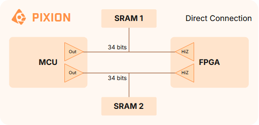
- Direct Connection: The MCU drives the pins while the FPGA stays in high-impedance (HiZ) mode, and vice versa. This setup is minimal and compact but requires precise timing to avoid any risk of short circuits.
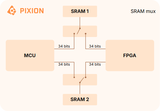
- High-Frequency Multiplexer on SRAM Pins: Place a high-frequency multiplexer on the SRAM pins to select whether the MCU or the FPGA is connected to the memory.
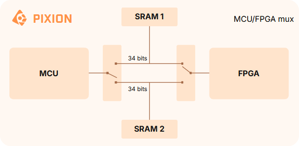
- High-Frequency Multiplexer on MCU and FPGA: Place a high-frequency multiplexer on the MCU (and FPGA) to select which memory is connected to the master
- Most Modular: All connections can be made. It is smaller and cheaper since fewer components are required. However, both the FPGA and MCU must dedicate 68 bits plus control signals and there is a risk of short between both.
- Safest Option: The MCU and FPGA can never be connected together, eliminating the risk of shorts. However, direct communication between the MCU and FPGA is not possible. This topology allows both SRAMs to be accessed by the same master (MCU or FPGA) simultaneously if needed.
- Direct Data Exchange: It’s impossible for one master to access both SRAMs at the same time, but direct data exchange between the MCU and FPGA is possible. This setup requires half as many pins (only 34) for the MCU and FPGA. This increases the risk of shorts, but handling this is easier than in the first situation.
- Direct Communication: It allows direct MCU-FPGA communication.
- Dual Access: Each master has the possibility to access both SRAMs at the same time if needed.
- No Short Risk: If the FPGA is properly set up (only once at the beginning), there is no risk of shorts between the MCU and FPGA due to bad timings or software bugs.
- Potential Delay: Depending on the implementation, there is a risk of adding a small fixed delay (1 clock cycle) between the MCU emission and the SRAM reception (to be confirmed).
- Pin Usage: While the MCU will only dedicate 34 bits instead of 68 for communication, the FPGA will need to use 102 pins.
Both have their advantages and drawbacks listed below:
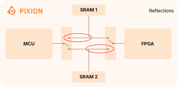
Personally, I favor the third option because I don’t need access to both SRAMs at the same time with one master, but I appreciate the possibility of bypassing the memory for direct MCU-FPGA communication. However, I’m concerned about reflections on the unconnected lines.
Maybe the best solution is to combine options two and three as shown in the picture below?
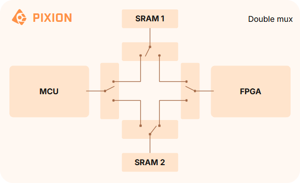
But wait a minute. This is becoming way too complex and bulky! There must be another way to do it. And actually, there is one.
We are using an FPGA. And this FPGA can act as our multiplexer, deciding whether we want to write the MCU or the FPGA bits to the SRAM. So, in the end, I came up with this architecture for the video buffer.
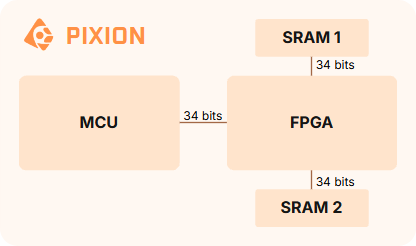
I like this solution, which I believe is simple and elegant, and it has the following pros and cons:
I’m curious to see how this final version of the architecture will perform, and I’m looking forward to sharing the results with you all. But first, we need to address other subparts of the architecture. Stay tuned for more updates as we continue to refine Pixion’s architecture!
Pix’